8-Bit SAP-1 CPU Architecture (Custom Logic Design)
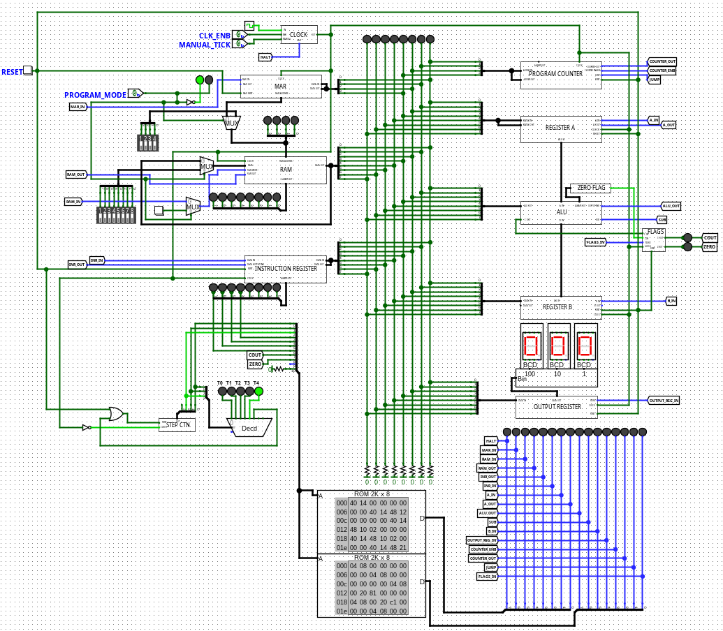
System Architecture
- CLK (Clock): The heart of the circuit. It ensures that all units of the processor run synchronously, meaning simultaneously and with a regular rhythm.
- Program Counter: Holds the RAM address of the next instruction to be executed. The counter is strictly designed to take an 8-bit value between 0-255. It increments by one after each instruction is processed to move to the next one.
- MAR (Memory Address Register): Temporarily holds the RAM address where the operation (read or write) will take place.
- RAM (Random Access Memory): The memory that stores the instructions of the written program and the data to be processed.
- Instruction Register (IR): Fetches and holds the next instruction from RAM. This instruction is then sent to the control unit to determine what needs to be done.
- Control Logic (OPCODE ROM, Step Counter, Decoder): The brain of the processor. It receives the instruction from the IR, decodes it, and decides which units need to operate to execute that instruction. It manages data traffic by sending signals to control lines (e.g.,
RAM_OUT,A_IN). - Register A & Register B: Memory cells where numbers are temporarily stored for arithmetic operations. ALU operations typically revolve around Register A.
- ALU (Arithmetic Logic Unit): The hardware that performs mathematical operations such as addition and subtraction. It takes the numbers in Registers A and B, processes them, and outputs the result back to the Bus.
- Flags (Carry & Zero): Reports the status based on the result of the ALU operation. If the result is 0, the Zero Flag is raised (becomes 1). If there is a carry out (meaning the calculation exceeds 8 bits), the Carry Flag becomes 1. This state is used in the processor’s decision-making mechanisms.
- Output Register & BCD: The output unit that takes the result of the operation and displays it in a human-readable format on 7-segment displays.
Working Logic
1. Fetch
The address in the Program Counter is sent to the RAM, and the corresponding data is fetched into the Instruction Register (IR).
2. Decode
The first 4 bits (Opcode) of the 8-bit data in the IR are sent to the control unit to determine what operation the system will perform.
3. Execute
The control unit physically executes the operation by opening the gates of the relevant modules (ALU, Register A/B) on the Data Bus.
Instruction Set
Processors only understand 1s and 0s. In an 8-bit processor, each instruction consists of 8 bits. In this SAP-1 architecture, the first 4 bits (opcode) state “What to do,” while the last 4 bits (operand) state “With what/At which address to do it.”
- 0000 (NOP): Do nothing, proceed to the next step.
- 0001 (LDA): Fetch the data at the given address from RAM and load it into Register A.
- 0010 (ADD): Fetch the data at the given address from RAM and add it to the current value in Register A.
- 0100 (STA): Take the result in Register A and save it to the specified address in RAM.
- 0101 (LDI): This instruction does not go to RAM. It directly takes the number written in the last 4 bits (Immediate value) and loads it into Register A.
- 0110 / 0111 / 1000 (JMP, JC, JZ): Disrupts the normal flow of the program and jumps to another address.
JC(Jump if Carry) andJZ(Jump if Zero) are critical for creating loops. - 1110 (OUT): Send the number in Register A to the display (Output Register).
- 1111 (HLT): Stop the clock signal, halt the program.
Machine Code Example: Sum of Sequential Numbers
The codes to be loaded into the 16-row memory (from 0 to 15) of the RAM:
1D 2E 4D E0 1E 2F 4E 79 60 F0 00 00 00 00 01 01Code Execution Breakdown:
First, we use the very last addresses of the RAM (addresses 13, 14, and 15) as “data storage” for the program to run:
- Address 13 (D):
00(We will keep the total here, initially 0) - Address 14 (E):
01(Our counter, the number that will increase in each step. Initially 1) - Address 15 (F):
01(Our constant 1. We will use it to increment the counter)
Instructions to Execute (Starting from Address 0):
- Address 0 - 1D (LDA 13): Load the value (Total) at RAM address 13 into Register A.
- Address 1 - 2E (ADD 14): Add the value (Counter) at RAM address 14 to the number in Register A. (Ex: In the first loop, 0 + 1 = 1)
- Address 2 - 4D (STA 13): Save the new total formed in Register A back to RAM address 13. (New total updated).
- Address 3 - E0 (OUT): Output the current total in Register A to the display.
- Address 4 - 1E (LDA 14): Now, fetch the value (Counter) at RAM address 14 into Register A.
- Address 5 - 2F (ADD 15): Add the “constant 1” value at RAM address 15 to the counter in Register A. (Counter becomes 2).
- Address 6 - 4E (STA 14): Save this new counter value (2) back to RAM address 14.
- Address 7 - 79 (JC 9): Carry Flag check. If the total exceeds the 8-bit limit (255), jump to address 9 to halt the program.
- Address 8 - 60 (JMP 0): Jump to the beginning of the program (address 0) and repeat the loop with the new counter.
- Address 9 - F0 (HLT): Halt the processor.